India's Semiconductor Dreams Take Flight: C-DAC Bengaluru Inaugurates Nation's Largest Pre-Silicon Chip Validation Facility
Bengaluru, India - In a significant stride towards bolstering India's indigenous semiconductor capabilities, the Centre for Development of Advanced Computing (C-DAC) today unveiled its state-of-the-art Pre-Silicon Chip Validation Facility at its Bengaluru campus. This sprawling facility, touted as the largest of its kind in the country, marks a crucial step in C-DAC's mission to empower Indian semiconductor design and manufacturing, reducing reliance on external entities and fostering a robust domestic ecosystem.
The inauguration ceremony, graced by dignitaries from government and industry, signifies a pivotal moment for India's ambitious semiconductor roadmap. The facility is poised to play a transformative role in the pre-silicon validation of complex integrated circuits (ICs), a critical and often time-consuming phase in the chip design lifecycle.
Addressing a Critical Bottleneck in Chip Design
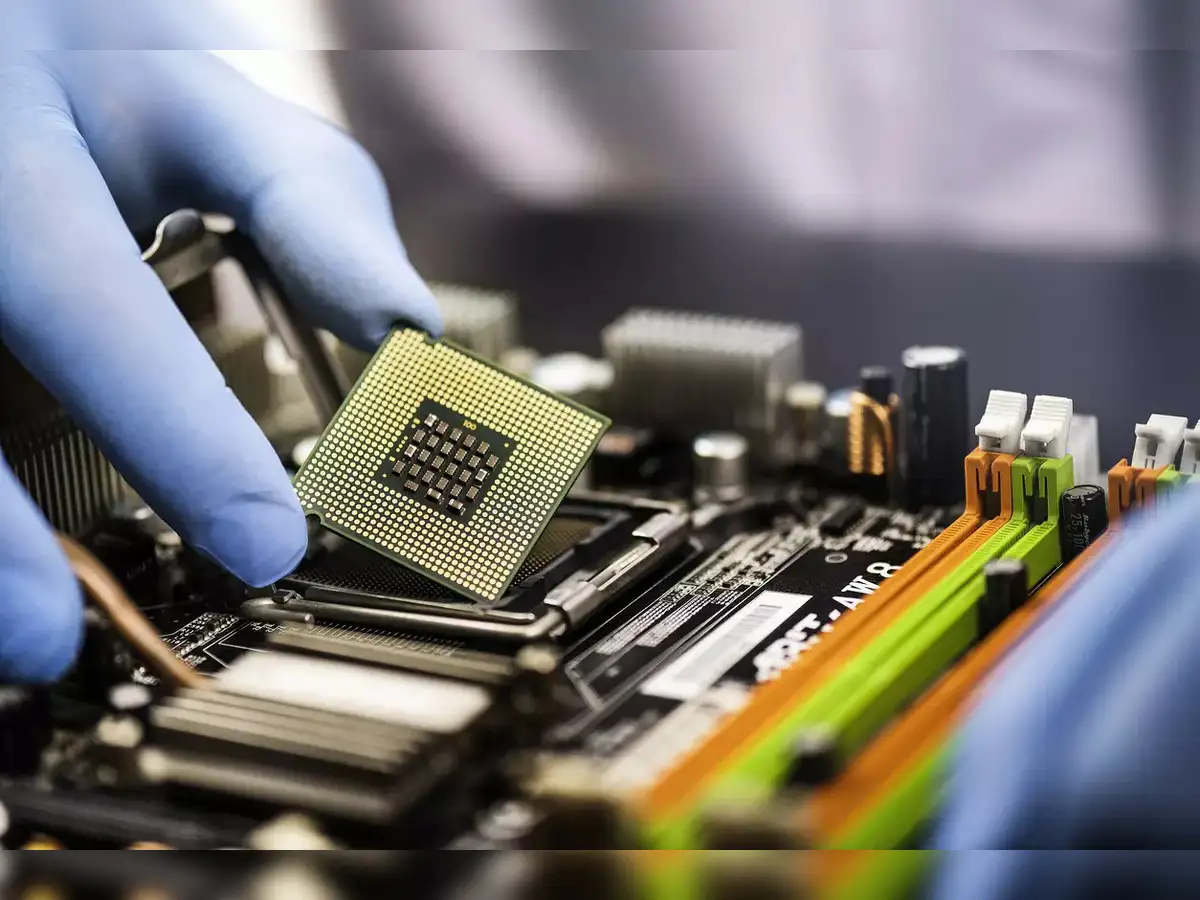
The pre-silicon validation stage is paramount to ensuring the functional correctness and performance of a chip before it is physically manufactured. This process involves rigorous testing and verification of the chip's design using sophisticated hardware and software tools. Identifying and rectifying design flaws at this juncture is far more cost-effective and time-efficient than discovering them after the chip has been fabricated.
Historically, India has faced challenges in possessing world-class pre-silicon validation infrastructure, often necessitating reliance on overseas facilities. The opening of C-DAC's facility directly addresses this bottleneck, providing Indian semiconductor companies, startups, and research institutions with access to cutting-edge resources and expertise.
A Comprehensive Suite of Capabilities
The newly inaugurated facility boasts a comprehensive array of advanced tools and technologies essential for the intricate process of chip validation. This includes:
* High-Performance Computing (HPC) Clusters: Powerful computing resources capable of running complex simulation and verification workloads at unprecedented speeds.
* Advanced Verification Tools: A suite of sophisticated software tools for functional verification, formal verification, and performance analysis, enabling exhaustive testing of design intricacies.
* Emulation and Prototyping Platforms: Hardware-based emulation and prototyping systems that allow for real-time testing of chip designs, simulating their behavior in a realistic environment.
* Specialized Test Equipment: Precision instruments and equipment for various testing methodologies, ensuring the integrity and accuracy of validation processes.
* Dedicated Team of Experts: A highly skilled team of engineers and researchers with extensive experience in semiconductor design and validation, providing crucial technical support and guidance.
Fostering Innovation and Self-Reliance
The facility is expected to be a catalyst for innovation, enabling Indian engineers to design and validate more complex and cutting-edge semiconductor chips for a wide range of applications, including:
* Artificial Intelligence (AI) and Machine Learning (ML): Accelerating the development of specialized AI chips for inference and training.
* Internet of Things (IoT): Enabling the creation of secure and efficient chips for a burgeoning IoT ecosystem.
* Automotive and Aerospace: Supporting the design of high-reliability chips for critical applications in these sectors.
* Telecommunications: Facilitating the development of next-generation communication chips.
* High-Performance Computing (HPC): Contributing to India's aspirations in supercomputing.
By offering these advanced capabilities locally, C-DAC aims to significantly reduce design cycles, lower development costs, and accelerate the time-to-market for Indian semiconductor products. This, in turn, will empower Indian companies to compete more effectively on the global stage and foster greater self-reliance in a strategically vital sector.
A Milestone in India's Semiconductor Mission
The establishment of this facility aligns perfectly with the Indian government's broader vision to establish a robust semiconductor manufacturing and design ecosystem within the country. Initiatives like the India Semiconductor Mission (ISM) have been launched to incentivize global and domestic players, and C-DAC's contribution is a vital piece of this puzzle.
"This facility is a testament to India's growing prowess in the semiconductor domain," stated a senior official at the inauguration. "By providing world-class pre-silicon validation capabilities, we are empowering our brightest minds to innovate and build chips that will power the future. This is a significant step towards achieving our goal of becoming a global hub for semiconductor design and manufacturing."
The C-DAC Bengaluru facility is expected to not only serve the needs of established players but also provide a crucial launchpad for burgeoning startups in the semiconductor space, democratizing access to advanced validation tools and expertise. This will nurture a new generation of semiconductor entrepreneurs and innovators, driving the next wave of technological advancements from India.
The opening of the nation's largest pre-silicon chip validation facility at C-DAC Bengaluru marks a pivotal moment, signaling India's unwavering commitment to building a self-sufficient and globally competitive semiconductor industry. This investment in critical infrastructure and expertise is poised to accelerate India's journey towards becoming a powerhouse in the world of microelectronics.

